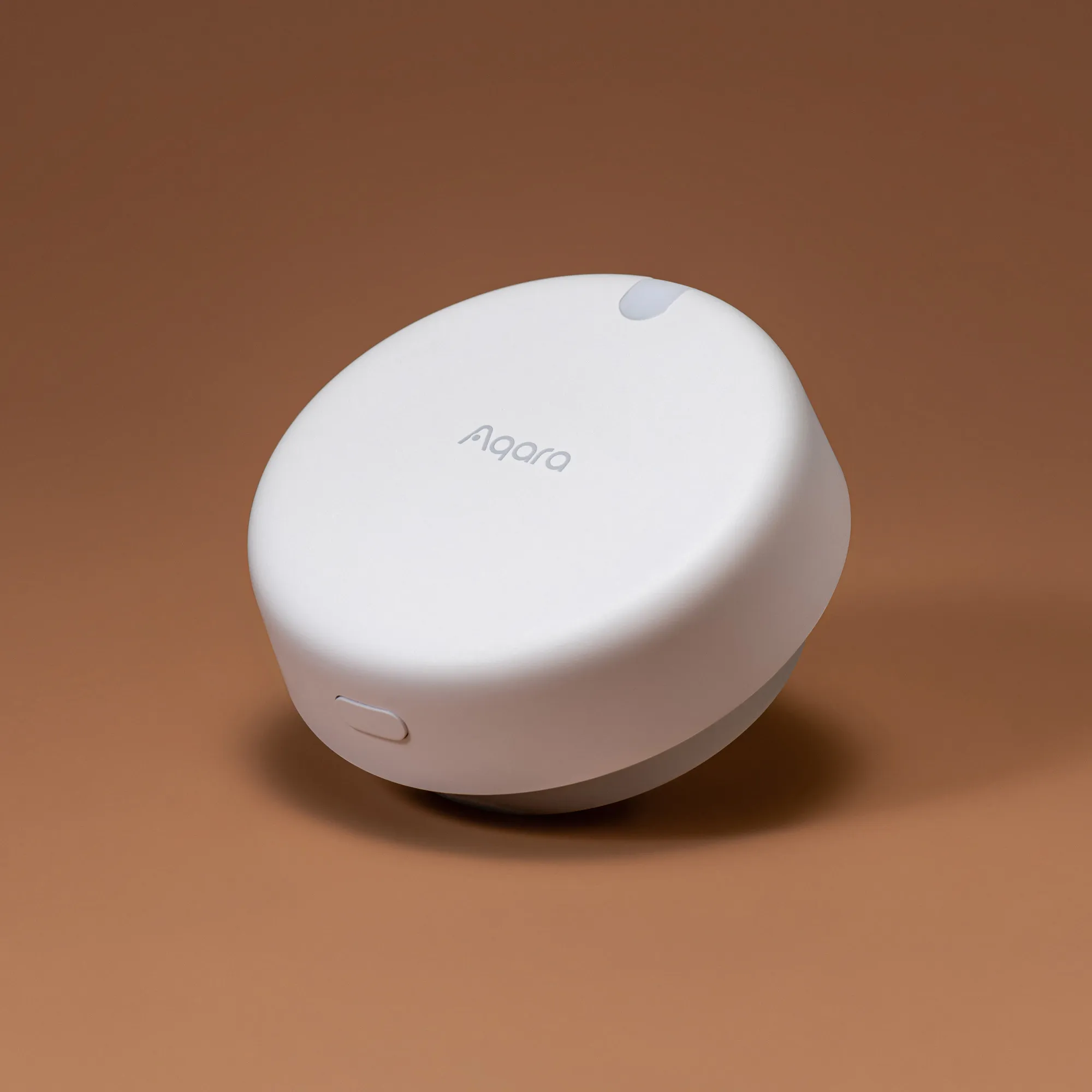
The Aqara FP2 is a pretty cool sensor intended for home automation. It is meant to be mounted in the corner of the room, and it can indicate to a home automation system whether there are people present in the space.
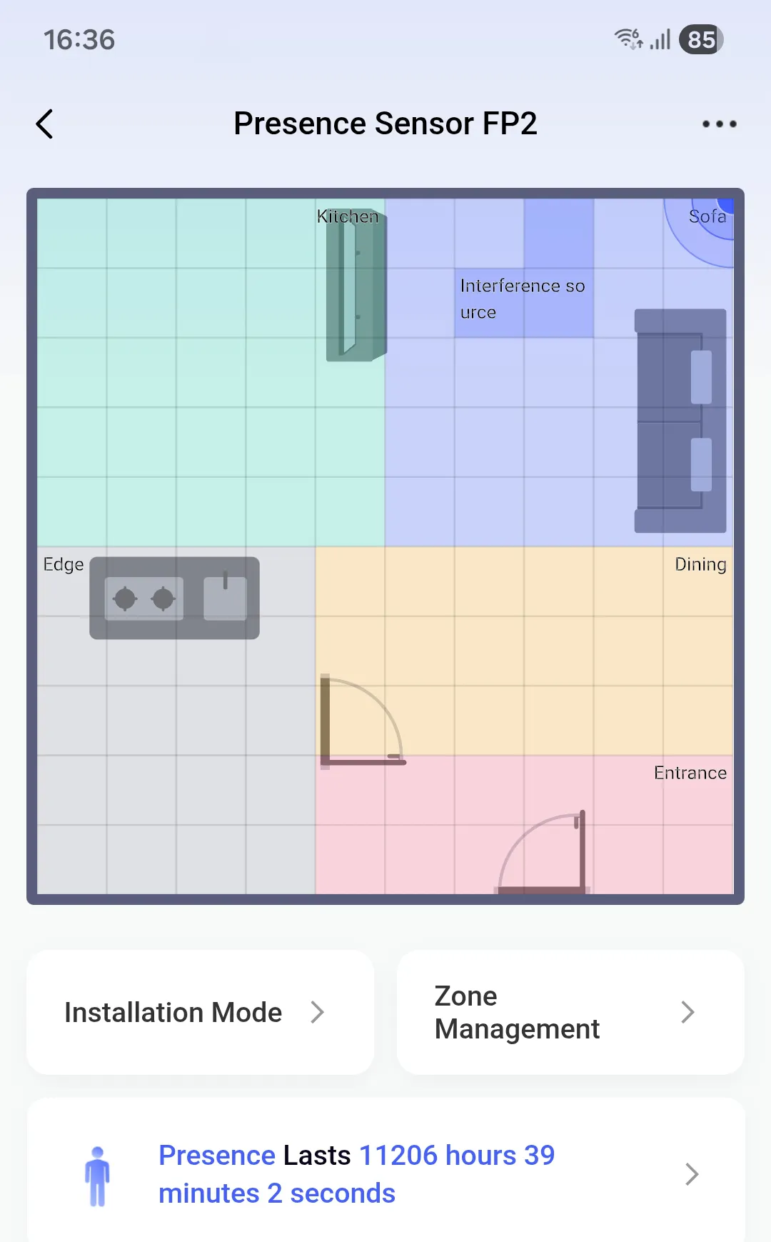
The cool thing about this sensor is it supports configurable zones. When opened in the app, you see a grid where you can see the positions of detected people. When you draw zones on the map, the sensor will indicate presence state for these zones individually.
It works by incorporating a MMWave radar. It operates at around 60GHz, where it blasts out radar chirps and looks at the way the signal bounces back to detect information about the scene it sees. We’ll get more into the details of this later as I find this stuff very interesting :)
Using the sensor with Home Assistant with stock firmare does come with some unfortunate downsides though.
While the sensor can be used day-to-day in a local only mode by pairing the sensor to Home Assistant through HomeKit, configuration and detailed information is only available though the Aqara app.
My goal with this project was to get custom firmware running on the device.
A first look at the hardware
The Aqara FP2 unit is relatively expensive, but you actually get a fair amount of hardware for your money.
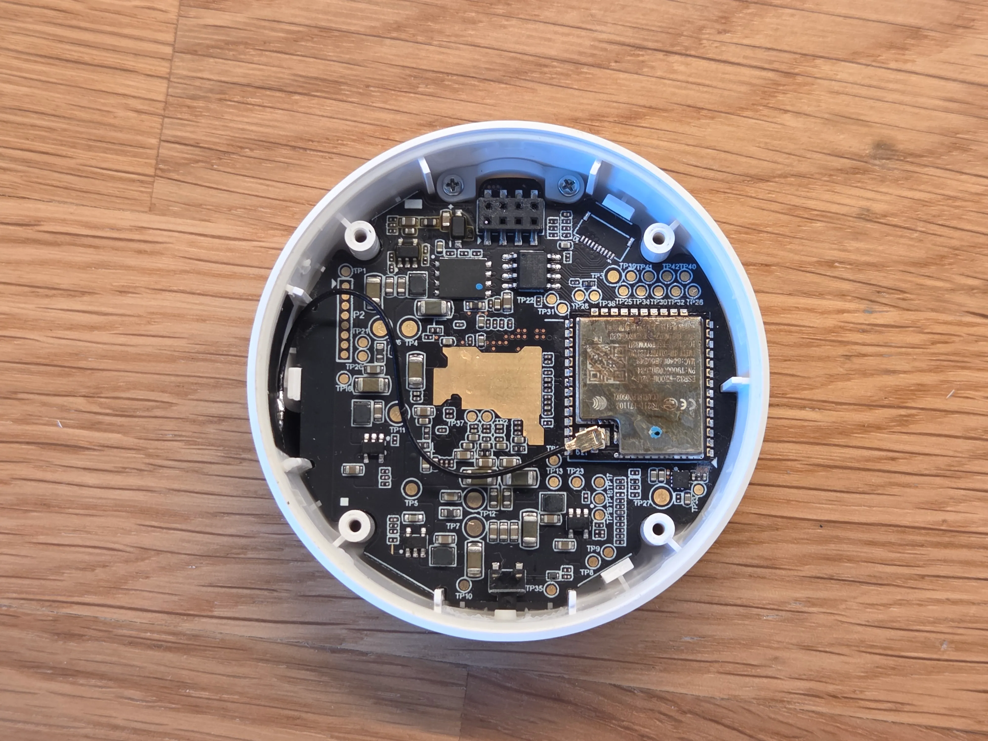
The back of the PCB is what you first see when you remove the back cover, and the most prominent component is a ESP32-WROOM-1U module. This is a good sign for me personally as it has a good open source SDK and is very nice to work with.
There is a fair bit more circuitry on the back of the PCB, but most of this stuff is fairly boring and can be summarized as:
- Flash for the ESP32
- Flash for the radar chip
- An accelerometer (we will get into this more later on)
- Most of the rest is power supplies for the radar chip, very boring stuff
A silicon heat transfer pad is mounted between the center of the PCB and the metal casing. Turns out the radar chip gets relatively hot, and the rear (made out of metal) is used as a heatsink.
We can also see a ton of test points and a few unpopulated connectors. Very interesting for us when we are reverse engineering.
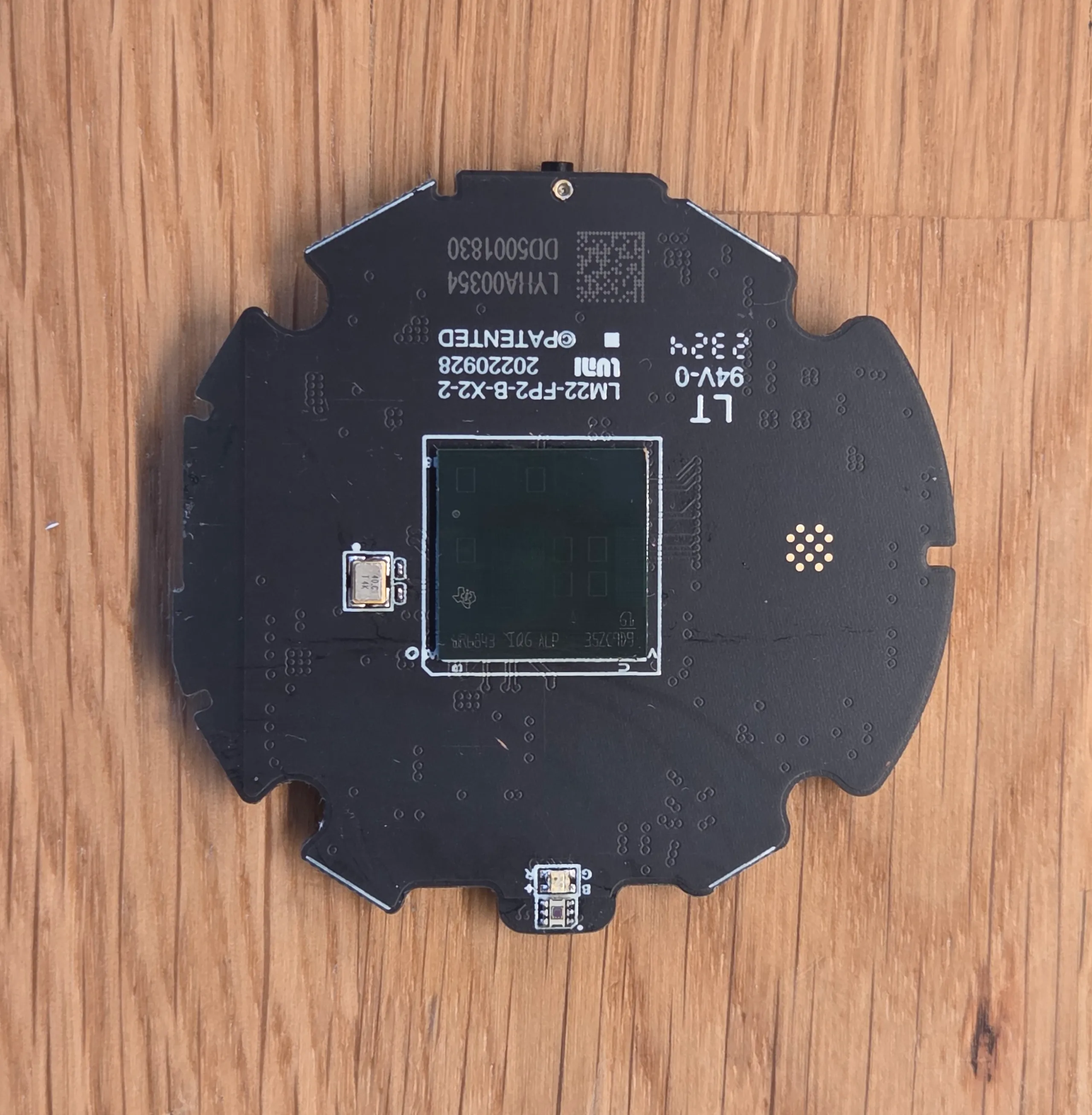
Pulling the PCB out of the front case reveals the actual business end of the device.
At the center is the MMWave chip itself, a IWR6843 by Texas Instruments.
The variant of the chip used here has a built-in antenna array, which makes incorporating this chip into your own products fairly easy, without having to deal with much RF magic.
You can see the 3 transmitter antenna elements faintly as an L shape, and the 4 receiver antenna elements as a square. This arrangement forms something called a MIMO SAR antenna array, which means we can math our way into virtual antenna elements. Briefly said, the more antennas we have the higher spatial resolution we can get from the radar.
Looking at the edge of the PCB we can also see two small chips. These are one RGB LED and one brightness sensor. These are used to indicate the state of the sensor and to sense the brightness of light in the room respectively. These both use the same lightpipe out of the case, so the light sensor cannot really be used while the LED is on without major interference.
Understanding the PCB
Just by looking at the hardware present in the device, we can already make some educated guesses about what components does what and how they fit together.
The ESP32 has the wireless hardware, so it will be the chip doing the talking to the outside world. The ESP32 will be connected to the IWR (radar) though some communication protocol, my initial guesses would have been UART or SPI, as these are common prococols for communicating between embedded chips, and both the IWR and ESP32 support them.
In order to get a better idea of how everything was connected, I desoldered the IWR and spent some time beeping out where most of its pads connect to.
[image of radar removed]
It turns out this whole PCB was a lot more boring than I had anticipated. The only connections between the ESP32 and the IWR are as follows:
- UART (TX/RX)
- Radar reset
A whole bunch of the IO and interfaces on the IWR are left not connected, with the exception of a pair of LVDS lanes which fan out to one of the unpopulated connectors on the back of the board. This LVDS interface can appearantly be used to stream out raw radar data from the sensor, and is meant to be used for development.
Knowing roughly how everything on the PCB is connected, we can reball and solder the IWR back on the device.
We now have a choice to make on how to proceed..
Crossroads
At this point we need to decide what path we want to take:
- We know enough about the PCB and pin assignments of the ESP and IWR that we can write our own firmware for both. Both have SDKs available publically, so this path is feasible
- Try to figure out how the ESP and IWR communicate to save ourselves from having to write the radar firmware
I went with option 2, if I decide I want to spend even more time on this project I can always just drop it and write my own. By understanding how they communicate from the factory, this would also let us flash our own firmware on the IWR from the ESP without having to connect to more tests points.
Probing the board
Knowing which pins the ESP32 and IWR is connected through gives us the ability to look at them talking together.
When reverse engineering something, there is a high chance you will be messing around with it for a while, so I find it it always worth it to make your setup as solid and convenient as possible.
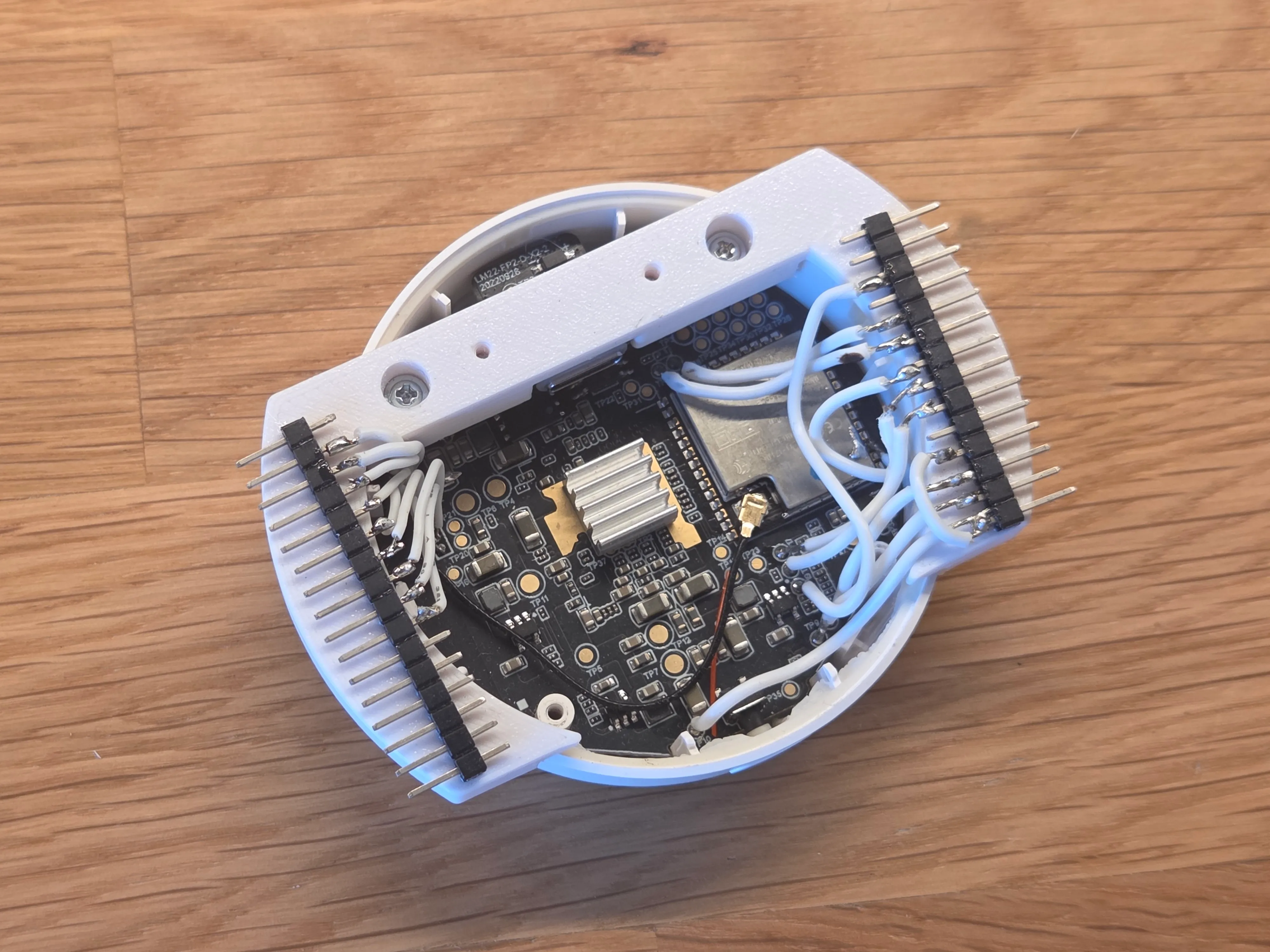
I designed and 3D printed out a plastic shim which I could screw into the front case. It provided mounting points for some pin headers I could use to break out any test point I needed access to + a mount for the USB C connector daughter board.
I also chucked on a small heatsink under the radar for good measure.
Sniffing communication
For actually reading out the serial data from the UART bus between the devices, I used a lovely little device called the Glasgow Interface Explorer.
It’s a small board with a FTDI chip, a small ICE40 FPGA, and some IO circuitry. Interesting hardware, but the real magic of this device comes from the software suite.
The ICE40 series of FPGAs has been fully reverse engineered, meaning they can be programmed and configured entirely with an open source toolchain.
The glasgow CLI tool and python library lets you describe hardware for the ICE40 FPGA using a Python DSL, then communicate directly with your gateware from Python. It’s an amazing concept and works really really well.
For sniffing the communication I just instantiated two UART RX modules in the FPGA, and could immediately handle the streams going in both directions in my Python code. Neat and very convenient!
Looking at the communication
I looked at the communication going back and fourth for a little bit. Spotted some structure, and clear correlation between the communication and things happening in front of the sensor.
I did realize fairly quickly though that reverse engineering the full protocol from just observing data over the wire was going to take a lot of work. At boot, there was a lot of traffic going back and fourth, and I would have to understand how everything fit together if I wanted to communicate with the radar from my own firmware
Changing gears, dumping ESP firmware
Since we know the pinout of the ESP32 module, connecting to its serial interface used for programming is fairly easy.
While the ESP32 is by no means a very secure chip, it does support stuff like firmware encryption and disabling the programming/debug ports which can make our lives a bunch harder. Always worth trying the simple way first, but we should be prepared that the manufacturer might not have made things easy for us…
Well, that was easy. No protections present, we were able to read out the unencrypted firmware image from the flash chip through the ESP32 serial interface.
Reverse engineering firmware
The ESP32 has Xtensa cores. Xtensa is a fairly niche ISA currently owned by Cadence.
Its niche is that the processor is licensed, and is meant to be customized. Evidently Espressif, the company which made the ESP32, licensed the IP and built a chip around it.
Luckily for us, Ghidra has very decent support for Xtensa.
[firmware loaded in ghidra] After unpacking the firmware image from the flash dump, we can start the puzzle.
Making progress
When reverse engineering firmware for MCUs, two places tend to be good starting points are:
- Look at the strings present in the firmware and where they are referenced from. These can give you a very good idea of what areas of the code do what.
- The firmware in a MCU interacts with the outside world through peripherals, which are controlled through registers in specific locations in memory. These registers are well defined for the chip model, and can be imported easily into Ghidra. Since we know, roughly how the chip behaves by observing it externally, this can be a very good starting point.
Luckily for us the firmware ships with a decent amount of logging code included. In our case this logging code often contained filenames and the name of the original functions, which made detangling the firmware a lot easier.
After some time grinding at the firmware in Ghidra from a few different directions, a clearer picture began to emerge.
The protocol is framed by:
| 0x55 0x00 0x01 | u8 | u8 | u16 | u8 |
| Static Sync Bytes | Sequence Number | Opcode | Payload Length N | Checksum |
Where the header checksum is a dead simple moduloed sum of previous header bytes.
This is followed by the payload itself and a checksum:
| N | u16 |
| Payload Data | CRC-16/MODBUS Checksum |
Nested within this, a attribute access protocol is used.
The opcode field in the header specifies:
| Opcode | Direction | Function |
|---|---|---|
| 0x01 | To ESP | Value Read Response |
| To Radar | Reverse Read Request | |
| 0x02 | To Radar | Write Request |
| 0x03 | Either | ACK |
| 0x04 | To ESP | Reverse Read Response |
| To Radar | Value Read Request | |
| 0x05 | To ESP | Value Report |
Notibly this allows:
- The ESP to read and write attributes on the Radar.
- The Radar to spontaineously request certain attributes from the ESP.
- The Radar to report changes to attributes.
- ACKs are used in both directions.
Within opcode payloads, a second envelope is used:
| u16 | u8 | variable |
| Attribute Identifier | Data Type (see below) | Data Type Payload (depending on Data Type) |
| ID | Name | Size | Encoding |
|---|---|---|---|
| 0x00 | u8 | 1 | Single byte, payload[0] |
| 0x01 | u16 | 2 | BE, payload[0] << 8 | payload[1] |
| 0x02 | u32 | 4 | BE |
| 0x03 | void | 0 | No data follows. Used for simple triggers/ACKs. |
| 0x04 | bool | 1 | payload[0] != 0 |
| 0x05 | string | 2 + N | Container. Length (u16 BE) followed by N bytes of ASCII string. Mainly used for logs seemingly. |
| 0x06 | blob | 2 + N | Container. Length (u16 BE) followed by N bytes of binary data. |
Attribute zoo
Following from here, my focus turned to writing a decoding/sniffing tool for the protocol.
It started out by dumping decoded frames with raw attribute data. This basic tool could then be used to try something on the physical device, see what data goes over the wire, try to spot correlations.
A few attributes were obvious, some arrived over the wire whenever motion was detected.
Other stuff like the flood of traffic happening on boot was more tricky to figure out on its own. This is where having the rough structure of the firmware mapped out in Ghidra really helps, I can map out how a binary blob or value is structured by reverse engineering the relevant attribute handler.
For work like this, investing time into improving your testing tools ALWAYS pays off many times over. Making it dead simple to capture a scenario in the app and see what traffic it results in over the bus immediately was critical.
Spending time writing proper docs is also worth it. I uploaded my raw docs here.
Some things, like the algorithm used to map accelerometer output to an enum number sent to the radar device required more RE effort. By looking at the way the disassembled code is structured, I get the impression the source code this compiled from was a bit of a hacky mess. Some sequences of floating point operations were also decompiled incorrectly by Ghidra, which was a real pain in the ass to map out.
Reimplementation
With the protocol and most important attributes figured out, it’s just a matter of writing alternate firmware for the ESP32 from here on.
I wanted this to work with HomeAssistant and be low mainternance, so I chose to do it as a ESPHome component.
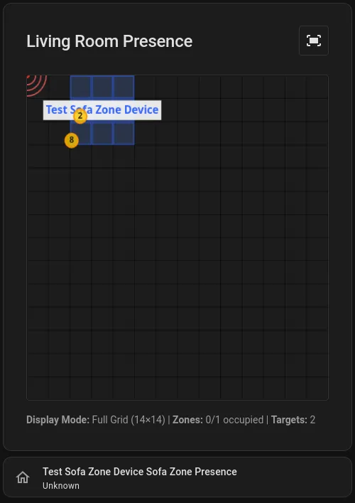
This part was relatively simple, and I finished off the project by implementing a nice HomeAssistant card which can visualize detected radar targets.
The project lives on
I don’t really have any interest in maintaining this long term, so lucky for me others have decided to fork my initial implementation to expand on it and maintain it. The most prominent one is esphome_fp2_ng by JameZUK. Thanks!
A personal note on LLMs
This reverse engineering effort was done with only selective help from LLMs late last year.
I have since given reverse engineering some other firmware a go, and the models have now progressed to the point where they can do so mostly autonomously, and very well.
Reverse engineering firmware like this was fun while it was still a useful skill, I suppose for now I still have something to offer on the hardware front, as AI hasn’t quite entered the physical realm yet :)
Hope I remain useful.